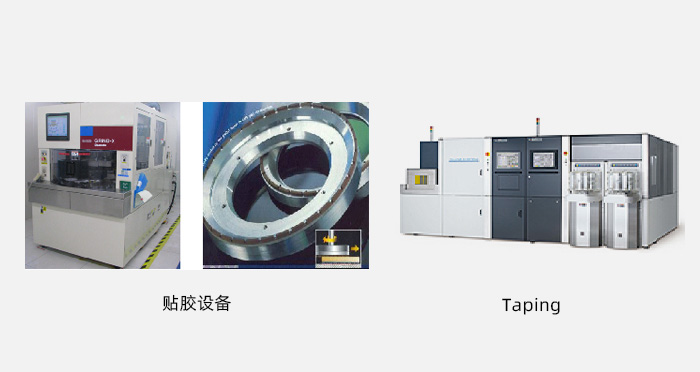
Use the manual diamond -made sand wheel (WHEEL), remove the silicon layer in the method of research on the WAFER crystal, and then thin the thickness of the WAFER to thinner the thickness of the customer through the two stages of roughly grinding & fine grinding.
For grinding thickness <120um demand products increase the fine grinding, that is, the polishing process, to obtain better processing surface roughness and eliminate remnants to increase the intensity.
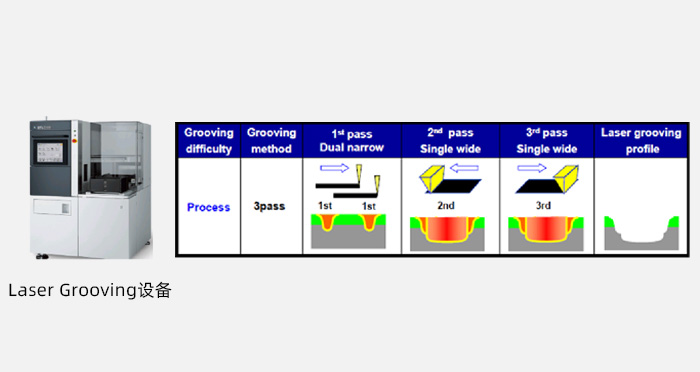
The LOW-K insulation film isolation of the Metal layer in a high-end process node wafer is low. Due to its low mechanical strength, if the ordinary cutting knife is used for cutting and processing, the risk of LOW-K film peeling and side cracking will occur. Such products need to implement LASER GROOVING (laser slot) to remove Low-K film and the corresponding metal layer to ensure the subsequent cutting knife cutting quality;
In the wafer manufacturing, the Metal layer has a CU layer. Because of its strong ductility, it is easy to cause cutting knife to cover and affect the cut quality. Such products need to execute Laser Grooving to remove the CU layer to ensure that the subsequent cutting knife cutting quality.
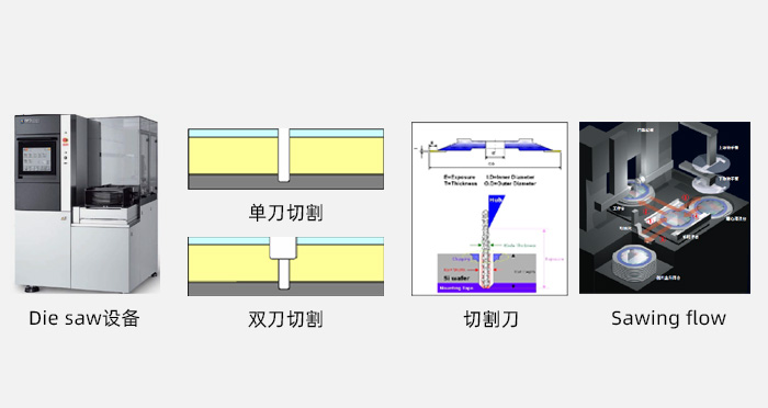
Use the cutting knife of the artificial diamond process, and cut the wafer as the customer's need Die size into a single grain in a high -speed cutting method to facilitate the subsequent DIE for the post -process;
Cutting is generally divided into single -knife cutting and double -knife cutting; relative to single -knife cutting, double -knife cutting the first knife cutting the cutting channel Metal layer to improve the impact of cutting channel materials on the blade, thereby improving the cut quality, so double -knife cutting into the current current Mainstream cutting mode.
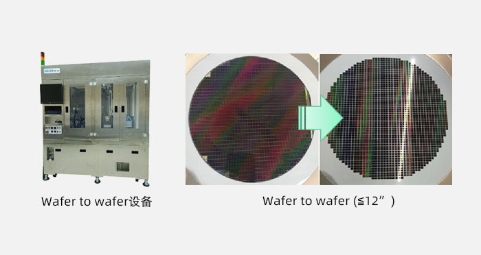
Dust -free workshop level: Class10, production capacity: 100kkea/m
After cutting the chopped wafer UV, separate the TAPE from the top acupuncture from the customer's needs, and then remove the DIE from the mouth absorption by the vacuum adsorption, and place it on the new empty TAPE for carrying it;
RW combines the two modes of INK & Mapping, and picked out the test of good products;
The RW machine records the position of each IC before picking up before, ensuring the traceability of the product;
The model of Quanliangpin's shipment ensures the compatibility of the post -process.
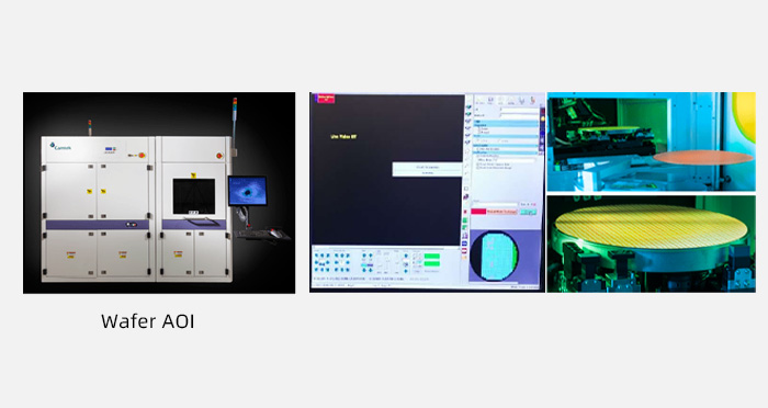
The DIE that is picked out is divided into good appearance and bad products through AOI automatic inspection equipment;
After the completion of AOI, generate AOI MAP, mark the bad products and bad products as different BIN CODE; use the AOI MAP to pick the device, screen out the bad products, and generate the final good product for shipment;
Wallopedic inspection capacity is 0.5um.
Address: No. 183 Fangzhou Road, Industrial Park, Suzhou City, Jiangsu Province
Copyright © King Long Technology(SuZhou) Limited. All rights reserved. Web design
![]()